Raymii.org

אֶשָּׂא עֵינַי אֶל־הֶהָרִים מֵאַיִן יָבֹא עֶזְרִֽי׃Home | About | All pages | Cluster Status | RSS Feed
My First PCB: Relay AND gate
Published: 20-01-2025 03:59 | Author: Remy van Elst | Text only version of this article
❗ This post is over one years old. It may no longer be up to date. Opinions may have changed.
Table of Contents
This is the result of my first attempt at learning KiCad during the Christmas break. I love the sound of a relay, so trying out these relay logic gates from the Usagi video and the information here on the MERCIA relay computer on a breadboard was fun, but a bit messy. No transistors or modern components, just relays, push buttons, resistors and LED's to show output. I've always wanted to make my own PCB. These simple relay logic gates are perfect to try out KiCad and actual PCB design, having never done that before. This short post shows you my first PCB, with all the beginner mistakes included.
Here is a PCBWay referral link for USD 5 credit.
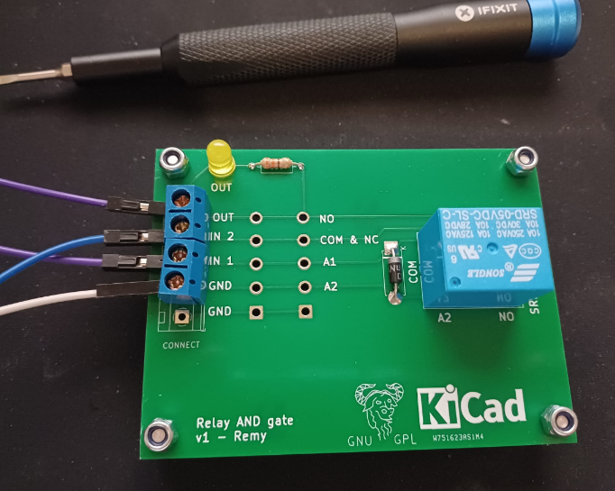
The finished PCB including soldered components. Screwdriver for scale
Please note that I'm not an expert at PCB design and this is my first time trying out KiCad. But oh boy did I have some fun learning. Receiving the first PCB in the mail was fun, soldering the components and then having it working the first time right way was even better.
Is it me, or, does everyone have this? When you've just finished the checkout process, you think of a few more changes that would have been nice to include?
Relay AND gate
This is a logic gate that should give a HIGH output when both inputs are HIGH. This design is before I learned about net classes, ground planes, design constraints, minimum trace sizes, custom footprints for a board with mounting holes and such. I also had the wrong symbol / footprint combo for the relay, so all my pins are manually coupled, no net names or automatically generated. Almost hand wired.
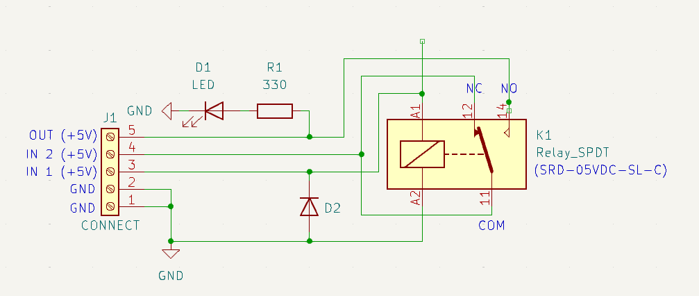
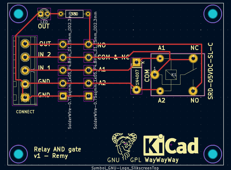
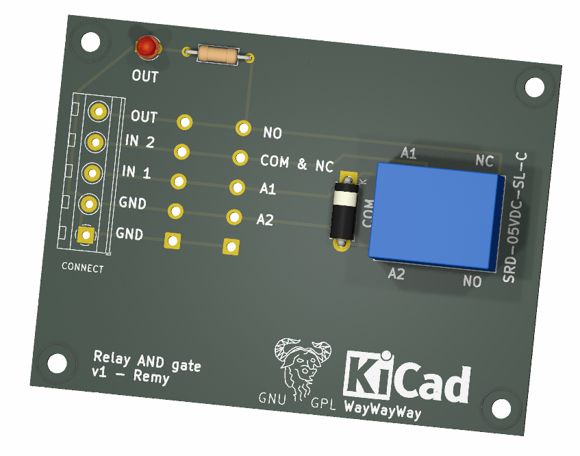
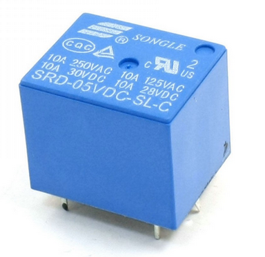
This is the relay I'm using. It's a 5V one, because that is what my Arduino UNO can provide power for, and more important, because I had a few of those lying around from earlier projects. They are a bit hard to use on breadboards, but with careful bending they do work.
The finished result is shown in the picture at the top of this page.
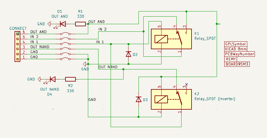
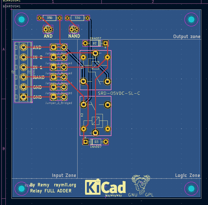
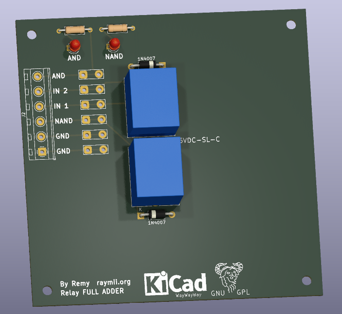
Relay NAND gate
A few attempts and a second relay later resulted in an extra output on the breadboard, the NAND (inverse of the AND). This PCB includes a ground plane, better design constraints, net classes and the correct symbol for the relay. I've also made a few custom components for the base board with mounting holes, the logo's and divided the board up into sections. The relays have a set position as well, so in total with this layout it should fit 8 or 9.
This PCB is bigger because I want to use it as a base for the other logic gates. It still fits in the 100x100mm size for PCBWay to get the cheapest price tier (USD 5 as of writing this article).
