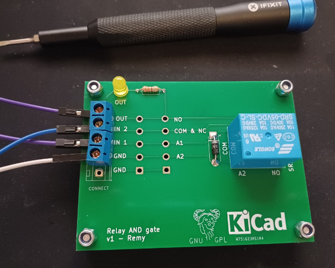
 > The finished PCB including soldered components. Screwdriver for scale Please note that I'm not an expert at PCB design and this is my first time trying out KiCad. But oh boy did I have some fun learning. Receiving the first PCB in the mail was fun, soldering the components and then having it working the first time right way was even better. Is it me, or, does everyone have this? When you've just finished the checkout process, you think of a few more changes that would have been nice to include? ### Relay AND gate This is a logic gate that should give a HIGH output when both inputs are HIGH. This design is before I learned about net classes, ground planes, design constraints, minimum trace sizes, custom footprints for a board with mounting holes and such. I also had the wrong symbol / footprint combo for the relay, so all my pins are manually coupled, no net names or automatically generated. Almost hand wired. 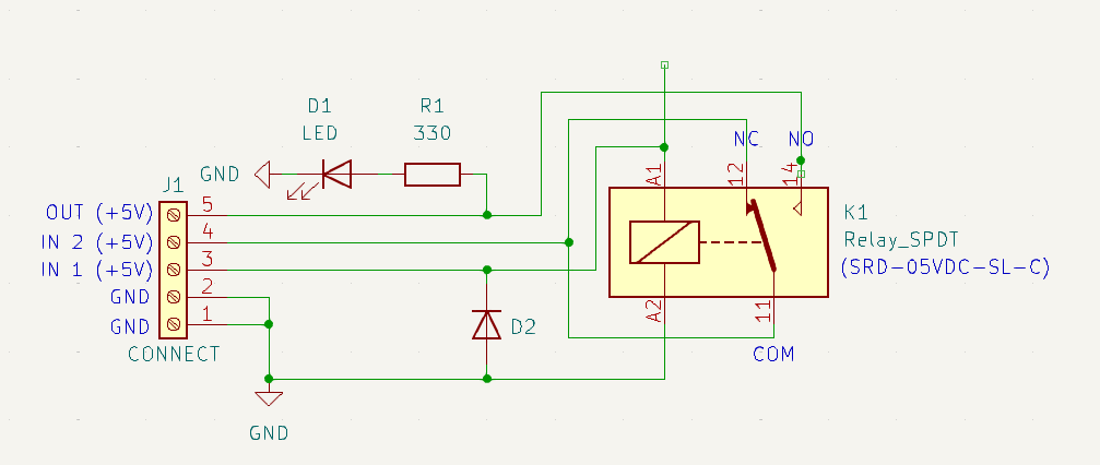 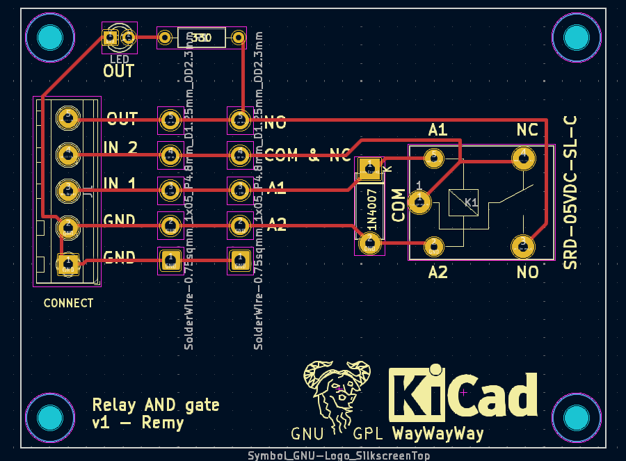 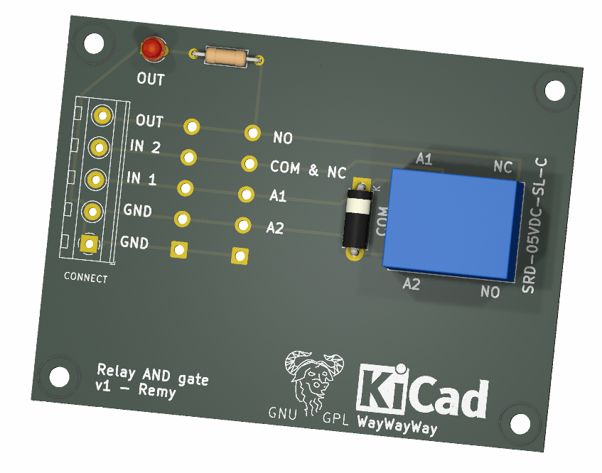 [This is the relay](https://web.archive.org/web/20250119182040/https://www.tinytronics.nl/en/switches/relays/relay-5v-250vac-10a) I'm using. It's a 5V one, because that is what my Arduino UNO can provide power for, and more important, because I had a few of those lying around from earlier projects. They are a bit hard to use on breadboards, but with careful bending they do work. 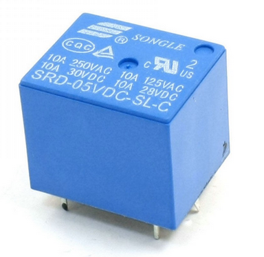 The finished result is shown in the picture at the top of this page. ### Relay NAND gate A few attempts and a second relay later resulted in an extra output on the breadboard, the NAND (inverse of the AND). This PCB includes a ground plane, better design constraints, net classes and the correct symbol for the relay. I've also made a few custom components for the base board with mounting holes, the logo's and divided the board up into sections. The relays have a set position as well, so in total with this layout it should fit 8 or 9. This PCB is bigger because I want to use it as a base for the other logic gates. It still fits in the 100x100mm size for PCBWay to get the cheapest price tier (USD 5 as of writing this article). 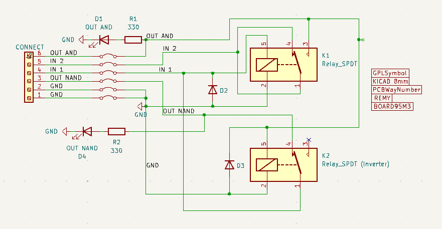 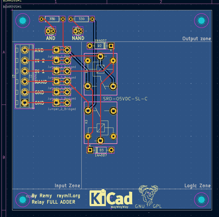 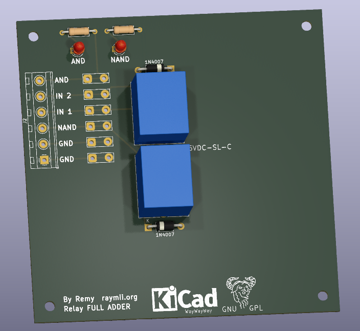 --- License: All the text on this website is free as in freedom unless stated otherwise. This means you can use it in any way you want, you can copy it, change it the way you like and republish it, as long as you release the (modified) content under the same license to give others the same freedoms you've got and place my name and a link to this site with the article as source. This site uses Google Analytics for statistics and Google Adwords for advertisements. You are tracked and Google knows everything about you. Use an adblocker like ublock-origin if you don't want it. All the code on this website is licensed under the GNU GPL v3 license unless already licensed under a license which does not allows this form of licensing or if another license is stated on that page / in that software: This program is free software: you can redistribute it and/or modify it under the terms of the GNU General Public License as published by the Free Software Foundation, either version 3 of the License, or (at your option) any later version. This program is distributed in the hope that it will be useful, but WITHOUT ANY WARRANTY; without even the implied warranty of MERCHANTABILITY or FITNESS FOR A PARTICULAR PURPOSE. See the GNU General Public License for more details. You should have received a copy of the GNU General Public License along with this program. If not, see